PCBA2Z Solutions · Mohali, Punjab+91 9115 79 3535 · info@pcba2z.com
PCBA2Z · PCB DESIGN SCHOOL

Best PCB Design Training Institute in Mohali · Chandigarh · Punjab.

PCBA2Z is an initiative by a group of qualified senior design engineers with strong practical experience in the field — professionals who don’t just design, but actually train engineers.

Learn through hands-on development of live projects, technical workshops, seminars, guest lectures and competitions — with a curriculum built around the real PCB design workflow.

Hands-on learningLive project workflowJob-oriented certificate course
Students learning electronics and PCB concepts
30–45 DaysStructured Basic & Advanced PCB Design training paths with practical learning.
Choose your path

Two focused PCB design courses.

Start with single-layer fundamentals or go deeper into double-layer PCB design and practical workflow.

Basic Course

Single Layer PCB Design

₹7,500
30 DaysSingle LayerCertificate

A structured entry into schematic capture, components, footprints, PCB layout and fabrication documentation.

  • New project creation & schematic capture
  • Component libraries and new component creation
  • PCB footprints in mm and mils
  • Single-layer layout, routing and documentation
  • Practical design workflow and DRC basics
Ask About Basic Course
Hands-on philosophy

A training environment built around doing, not just watching.

PCBA2Z is positioned as a practical learning environment where budding engineers can work through the complete PCB design journey. The aim is to connect schematic thinking, physical layout, fabrication awareness and project execution so learners develop a clearer understanding of how real boards come together.

01

Live Projects

Learn through development-focused examples and project workflows.

02

Workshops

Hands-on sessions designed to turn theory into practical confidence.

03

Seminars

Exposure to technical concepts, industry context and new ideas.

04

Competitions

Practice, build and demonstrate technical understanding.

Complete curriculum

From schematic capture to fabrication data.

The curriculum combines foundational PCB knowledge with actual design workflow and output generation.

01

Schematic Capture

Build the logical foundation of a PCB before moving into physical placement and routing.

New Project CreationSingle and multiple sheet designsConnectivity of all sheetsSelecting components from LibrariesMaking New ComponentsCheck DRCBill of Material CreationNet-list creationIntroduction to Through-hole and SMT componentsStudy of electronics component datasheetsPCB Footprints in mmPCB Footprints in mils
02

PCB Layout

Turn the schematic into a manufacturable physical board through component placement and routing.

Import Net-list into PCB PackageSelect PCB footprints from LibraryMake New Components / PCB FootprintsSelection of LayersSelection and Placement of ComponentsRouting — TracksSingle Layer PCB DesignsDouble Layer PCB DesignsInter-communication toolsCross probing
03

Introduction to PCBs

Understand the board itself — what it does, what it is made from and how it is manufactured.

Functions of PCB’sClassification of PCBTypes of PCB’sBase materialParts of PCBPCB Manufacturing TechnologySteps in PCB FabricationPCB Design Process
04

Gerber Data Generation

Finish the design workflow with fabrication-ready output concepts.

Gerber Data GenerationPanelizationEdit GerberFabrication documentation
Campus workshops

Learning goes beyond the classroom.

PCBA2Z also conducts workshops focused on printed circuit board design. Students get exposure to PCB functions, types, classifications, base materials and the design of single- and double-layer boards using CAD.

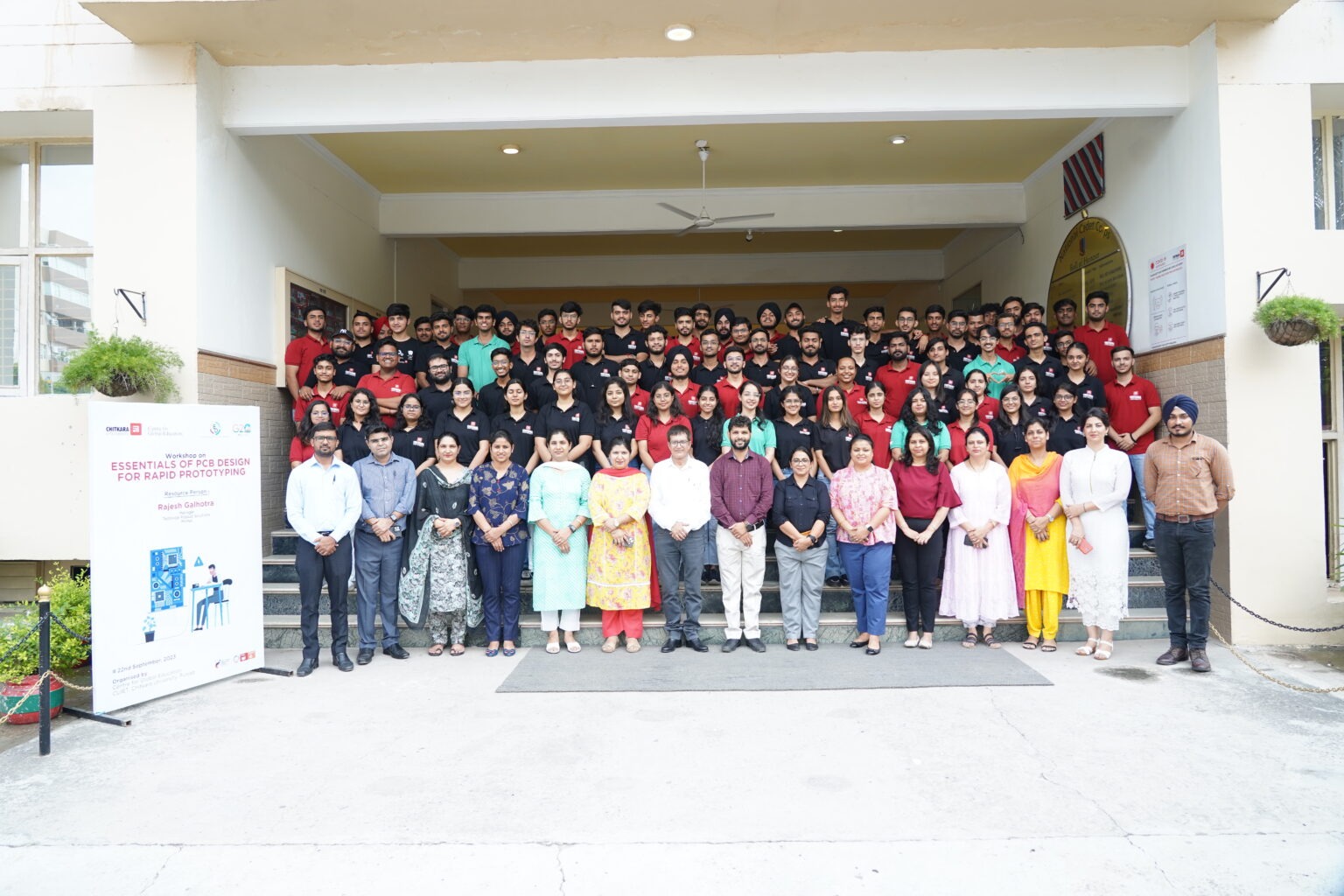
Workshop at Chitkara University

Essentials of PCB Design for Rapid Prototyping

Real workshop moments, preserved in their original proportions — no cropping.

Workshop at Chitkara University — full group workshop image
Workshop at Chitkara UniversityFull-width showcase image
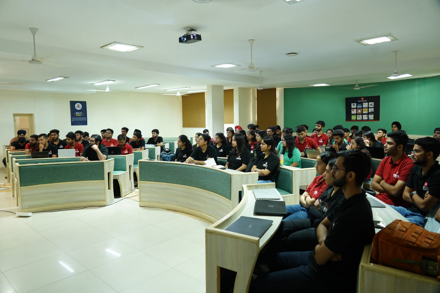
Workshop at Chitkara University — classroom session
Chitkara University · Workshop session
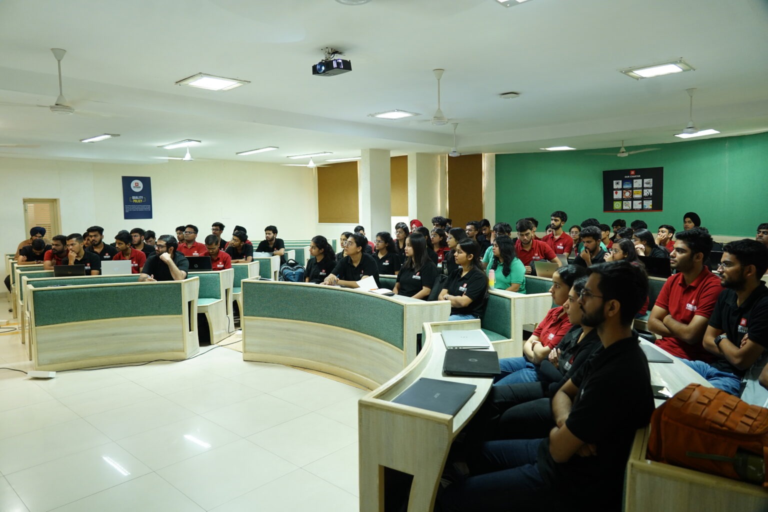
Workshop at Chitkara University — student session
Chitkara University · Student learning
Workshop at Chitkara University — practical learning
Chitkara University · Practical workshop
Workshop at RIMT University

Hands-on PCB design exposure

Three corrected RIMT workshop images supplied for the demo.

Workshop at RIMT University — classroom session
RIMT University · Workshop session
Workshop at RIMT University — student session
RIMT University · Student learning
Workshop at RIMT University — classroom interaction
RIMT University · Classroom interaction
We are flexible to incorporate changes as per institute requirements and look forward to long-term association for technical workshops and training programs.
Workshop outline

What students cover during a workshop.

A compact, practical introduction to the printed circuit board workflow.

PCB

Introduction to PCB’s

Understand the role and physical structure of a printed circuit board before beginning layout design.

  • Classification of PCB
  • Base material
  • Parts of PCB
  • PCB Manufacturing Technology
  • Steps in PCB Fabrication
SCH

Schematic Capture

Learn the logical design process and prepare the foundation for physical PCB implementation.

  • New Project Creation
  • Single and multiple sheets
  • Connectivity of all sheets
  • Component libraries and creation
  • DRC, BOM and Net-list
  • Datasheets, Through-hole and SMT
CAD

PCB Layout

Move from net-list and footprints to placement, layer selection and routing.

  • Import Net-list
  • Footprints from library
  • New PCB footprints
  • Layer selection
  • Component placement
  • Routing and cross probing
GER

Gerber Data Generation

Learn the output side of the process so designs can be prepared for fabrication.

  • Gerber data generation
  • Panelization
  • Edit Gerber
  • Fabrication-ready documentation concepts
PCBA2Z founder and trainer
Founder · TrainerPCBA2Z Solutions
Learn from practical experience

Training led by engineers who work with the discipline.

PCBA2Z presents the training initiative around qualified senior design-engineering experience — with a focus on making the concepts usable, not merely theoretical.

The program is structured for learners who want a guided path through schematic capture, PCB layout, fabrication concepts and practical project development.

01

Practical

Hands-on concepts with project-led learning.

02

Technical

Design workflow, documentation and fabrication awareness.

03

Career-oriented

Build a base for PCB design and fabrication roles.

Eligibility

Who can join?

The program is open to a wide range of learners with an electronics or technical background.

10+2 / ITI

Students beginning their electronics journey.

Diploma

Technical diploma learners building practical skills.

B.E. / B.Tech / B.Sc / M.Sc

Engineering and science students wanting design depth.

M.E. / M.Tech / Technicians

Advanced learners, working technicians and electronics professionals.

Also welcome: students with little knowledge of electronics can also join and learn progressively.
Course outcome

What students can explore after the course.

On completion, students can explore different aspects of printed circuit board design and fabrication and build a stronger foundation for work in PCB designing and fabrication.

  • Understand different types of PCBs and schematic design
  • Learn rules for schematic entry and component layout methods
  • Practice placement rules and routing techniques for single-sided boards
  • Understand post-processing and fabrication documents
  • Design and fabricate project PCBs using a clearer workflow
Why PCB Design & Manufacturing?

Printed circuit boards are core components in electronics, from domestic gadgets to industrial products. PCB design helps translate electronic circuits into reliable physical hardware. A thoughtful design process can reduce design errors and improve manufacturability.

It Pays HandsomelySpecialized engineering capability.
Many Job RolesDesign, layout, CAM and documentation.
Growing FieldElectronics product development continues to expand.
ChallengingDetailed work for technical minds.
Big OrganizationsOpportunities across engineering ecosystems.
Excellent CommunityLarge online learning and engineering community.
Easy to LearnProgressive skill development is possible.
Practical SkillUseful for projects and manufacturing workflows.
Career prospects

Where can PCB design skills take you?

PCB design is a specialized engineering path with a range of possible roles.

CAD

PCB Designer

Build schematics, footprints, layouts, routing and design documentation.

ENG

Electronics Design Support

Bridge circuit decisions with their physical implementation.

MFG

PCB Fabrication / CAM

Work closer to manufacturing, Gerber data and vendor workflows.

Expected remuneration listed by PCBA2Z: ₹3.4 lakh / year to ₹5.3 lakh / year for freshers working in this field. This is an indicative estimate published by the institute, not a guaranteed salary.
Student success stories

What learners value about the journey.

One published testimonial is shown exactly as supplied; the remaining cards are clearly marked as demo feedback highlights rather than attributed reviews.

★★★★★ · Rated 5 out of 5
The hands-on training at PCBA2Z was key to my career change to PCB design. The guidance I received was exceptional!Mohit Bagari · PCB Designer
DEMO FEEDBACK HIGHLIGHT
Hands-on practice makes the PCB design workflow easier to understand than theory alone.Non-attributed demo highlight · Practical learning theme
DEMO FEEDBACK HIGHLIGHT
The journey from schematic to footprint to routing creates a much clearer picture of how a real board is built.Non-attributed demo highlight · Course learning theme
DEMO FEEDBACK HIGHLIGHT
Workshop exposure helps learners connect classroom concepts with actual engineering environments.Non-attributed demo highlight · Workshop theme
DEMO FEEDBACK HIGHLIGHT
Understanding Gerber and fabrication documentation makes the design process feel much more complete.Non-attributed demo highlight · Fabrication theme
DEMO FEEDBACK HIGHLIGHT
A guided curriculum helps beginners build confidence without getting lost in the details too early.Non-attributed demo highlight · Beginner theme
For the live website, replace the demo highlight cards with verified student reviews or institute-approved testimonials before launch.
Before you enrol

Training FAQ.

Quick answers to the questions learners usually ask before starting.

Yes. The institute states that students with little electronics knowledge can join. The learning path starts with project creation, components and schematic capture before moving into layout.
The Basic Course focuses on single-layer PCB design over 30 days. The Advanced Course focuses on double-layer PCB design over 45 days.
Yes. The training proposition is built around hands-on development, practical workshops and live-project-oriented learning.
Yes. This page showcases workshop activity at Chitkara University and RIMT University, and the institute states that workshop programs can be adapted to an institute’s requirements.
Use the enquiry button to open the contact page, or call +91 9115 79 3535.
Ready to start?

Build your first serious PCB workflow.

Ask about course schedules, institutional workshops or the next training batch.

Get Training InfoCall Now