Where circuit ideas become real boards.
Design it. Validate it. Fabricate it. Learn the workflow from people who understand the engineering, sourcing and manufacturing path behind a PCB.
One brand. Four clear ways to work with us.
Whether you're shipping a product, sourcing a board, learning PCB design or running a workshop, the site now takes you straight to the right next step.
PCB Design Services
Schematic capture, footprints, placement, routing, DRC, BOM and Gerber-ready output.
Explore design →PCB Fabrication
Single, double, multilayer and flexible PCB sourcing through selected manufacturing vendors.
See fabrication →PCB Design Training
Hands-on, job-oriented PCB learning built around live projects and practical manufacturing knowledge.
See courses →Project Kits & Components
Electronics components, project kits and practical hardware for students and makers.
View kits →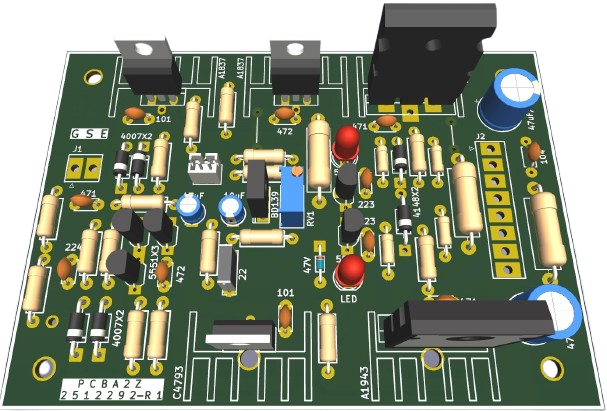
Not just pretty traces. A path to fabrication.
PCBA2Z describes a senior-led workflow spanning PCB layout, fabrication, assembly and component sourcing. The redesign turns that story into a more transparent project journey.
Turn your circuit intent into a clear board requirement.
Capture, place, route and review against design rules.
Generate fabrication data, BOM and manufacturing documentation.
Compare supplier capability, cost, material and timing.
Learn the tools. Understand the board. Build something you can show.
₹7,500
Single-layer PCB Design • 30 days
₹15,000
Double-layer PCB Design • 45 days
Products and boards with a story behind them.
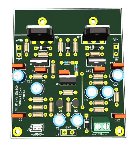
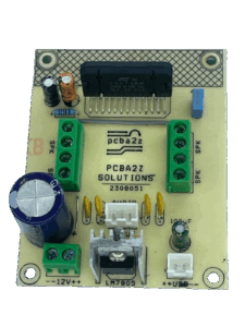
From engineering teams to classrooms.
Startups
Prototype and product teams that need a dependable design-to-fabrication path.
Engineers
Design, DFM coordination and vendor communication without another layer of complexity.
Institutions
Hands-on PCB workshops, seminars and practical training experiences.
Makers & Buyers
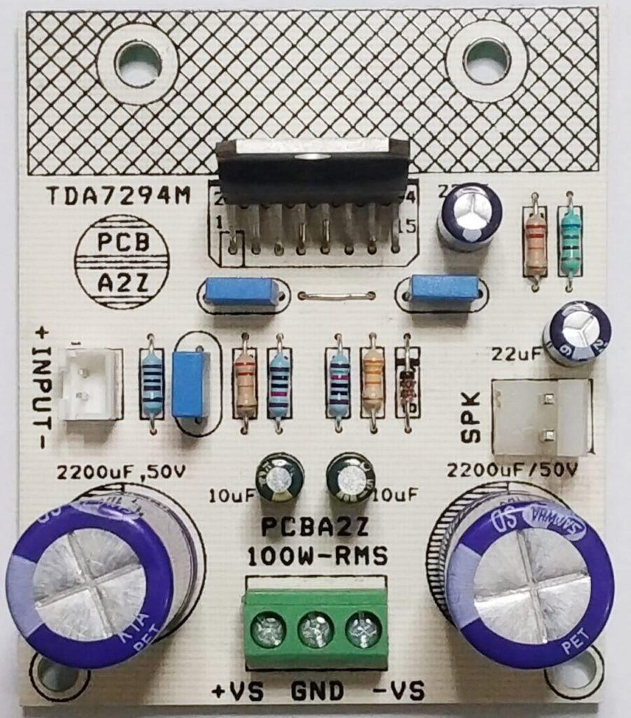
Ready-made boards, project kits and components through the store experience.
Procurement knowledge changes engineering decisions.
The current PCBA2Z story emphasizes experience not only in PCB layout but also sourcing, vendor development, inventory and materials. That makes the business especially relevant when engineering choices have to survive cost, lead-time and manufacturing realities.
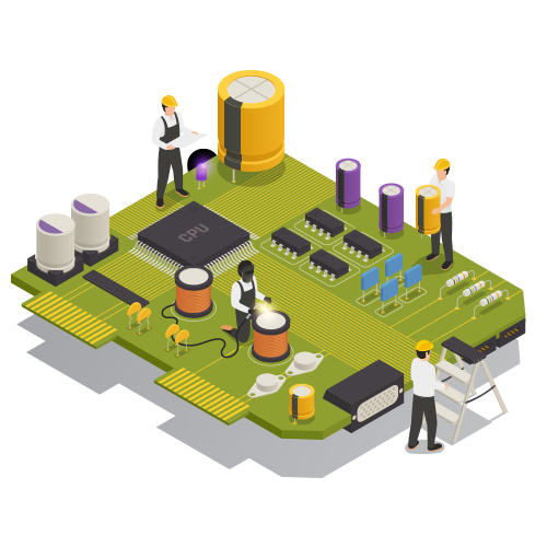
Learning looks better when it happens hands-on.
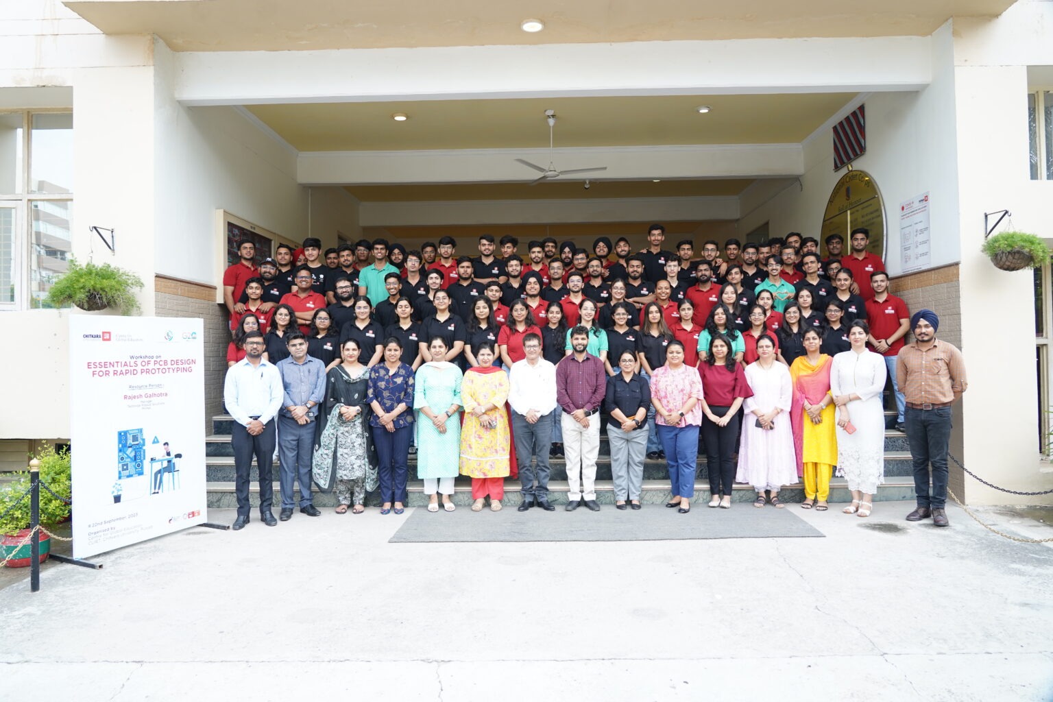
Essentials of PCB Design for Rapid Prototyping
Workshop imagery supplied from the existing PCBA2Z site assets.

Hands-on classroom sessions
Practical workshop sessions for learners and engineering audiences.
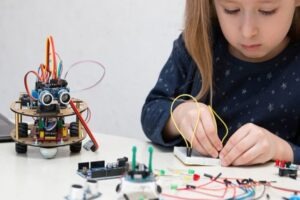
Build while you learn
Electronics projects give students a tangible way to understand circuits and boards.
Send the board problem. Start with the right question.
Upload a schematic, Gerbers, BOM or simply tell us what you are building. The demo RFQ flow is ready for a real integration later.