pcba2z positions itself at the intersection of PCB design, fabrication coordination, component sourcing and practical training.

The current PCBA2Z website describes its team leader as having more than 20 years of technical experience across PCB layout design, PCB fabrication, PCB assembly and component sourcing.
It also cites previous experience at Continental Device India Limited (Deltron Division) in a materials-oriented role covering sourcing, price reduction, inventory, vendor development and raw-material planning.
Technical experience stated by the current site.
Design knowledge converted into practical learning.
Vendor, cost and timing considerations inform the workflow.
OrCAD, Altium, Proteus and KiCad referenced.
Design choices influence manufacturing, sourcing, testing, cost and lead time. That is the story the new site makes visible.
Clarify circuit intent, constraints, performance and manufacturing goals.
Capture schematic, choose footprints, place components and route the PCB.
Run design checks, inspect documentation and prepare the manufacturing data.
Compare vendor capability, quality, timing, materials and cost.
Coordinate fabrication and assembly through selected suppliers.
PCBA2Z's education proposition is built around practical projects, workshops, seminars, guest lectures and competitions rather than theory alone.

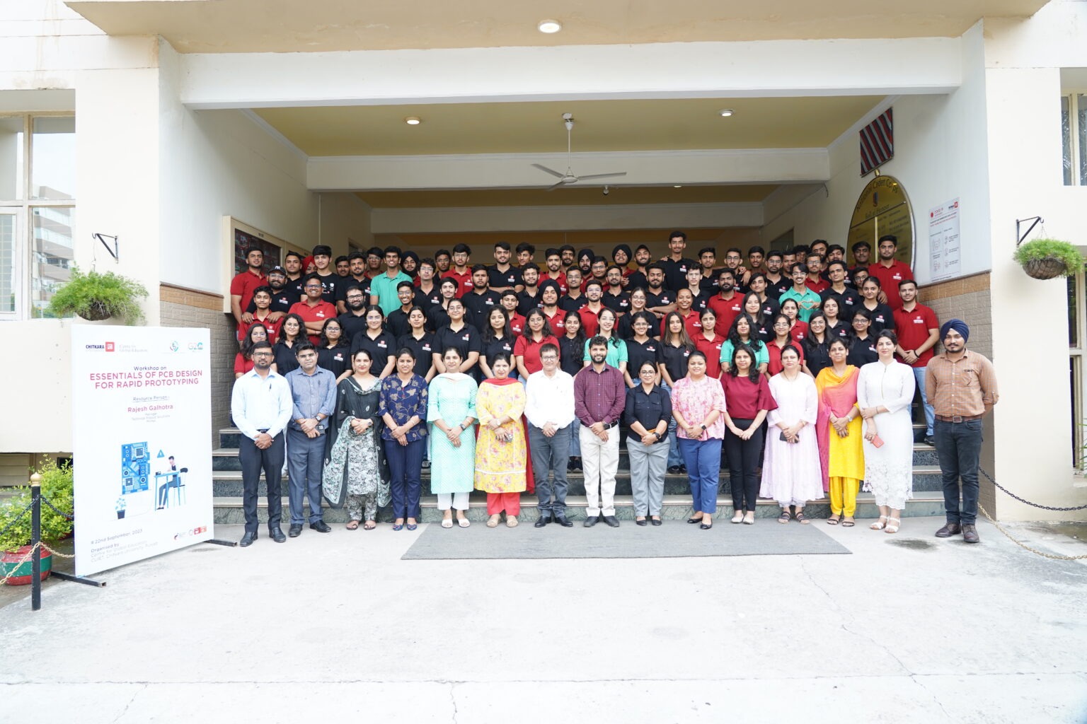
Existing PCBA2Z workshop imagery used in this redesign.
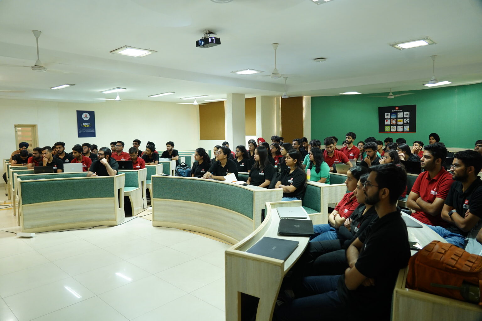
Large-group training environments built around hands-on learning.
Workshops for students and technical learners.
Pick the path that matches what you're trying to achieve and start the conversation.